PIR Sensor
- Rajkumar Sharma
- 41.406 Views
- advanced
- Tested
- SKU: EL36094
- Quote Now
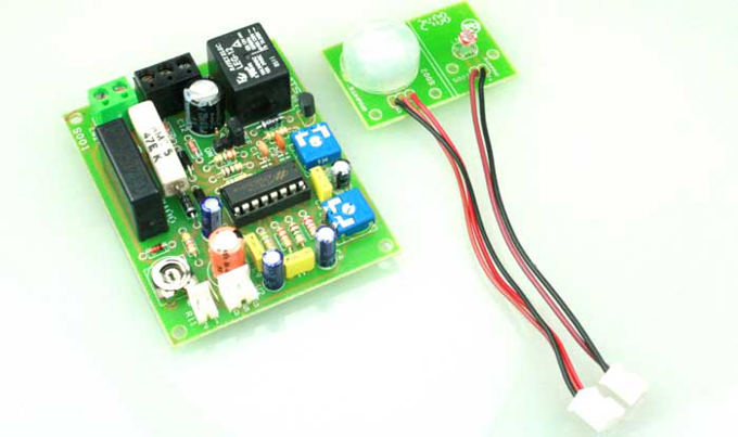
This project is an automatic PIR sensor.
Description
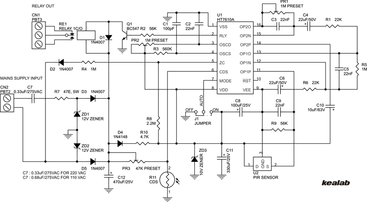
Project is based on Holteks IC HT7610A, which is a CMOS LSI chip designed for use in automatic PIR lamp, flash or buzzer control. It can operate in 3-wire configuration for relay applications. In our project we have used relay instead of Traic to connect any kind of load in output, HT7610B IC is suitable for traic and HT7610A for Relay application. The chip is equipped with operational amplifiers, a comparator, timer, a zero crossing detector, control circuit, a voltage regulator, a system oscillator, and an output timing oscillator.
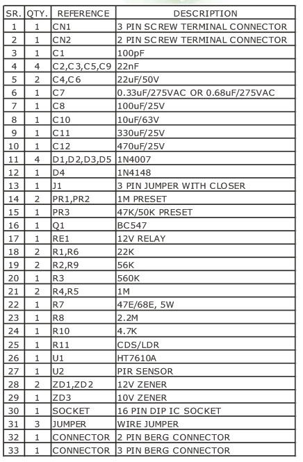
Its PIR sensor detects infrared power variations induced by the motion of a human body and transforms it to a voltage variation. If the PIR output voltage variation conforms to the criteria (refer to the functional description), the lamp is turned on with an adjustable duration. The circuit doesnt required step down transformer and can work directly by applying 110V AC or 220V AC (Capacitor C7 needs to change for 220V AC (0.33uF/275V) and 110V AC (0.68uF/275V)
Features:
- Supply Input 110V or 220V AC ( Capacitor Value needs to Change)
- No Step Down transformer required
- IC Operating voltage: 5V~12V
- Load Current 80mA when relay is on.
- Standby current of the IC: 100uA
- On-chip regulator
- Adjustable output duration
- 40 second warm-up
- ON/AUTO/OFF selectable by MODE pin
- Override function
- Auto-reset if the ZC signal disappears over 3 seconds
- On Board Relay to connect output Buzzer or Flash
- On Board LDR to Detect Day/Night operation
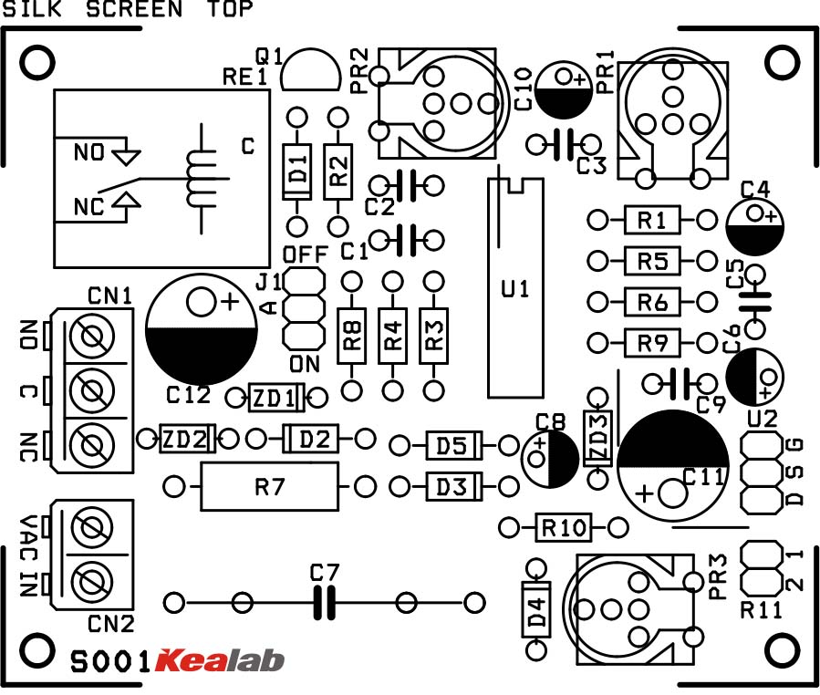
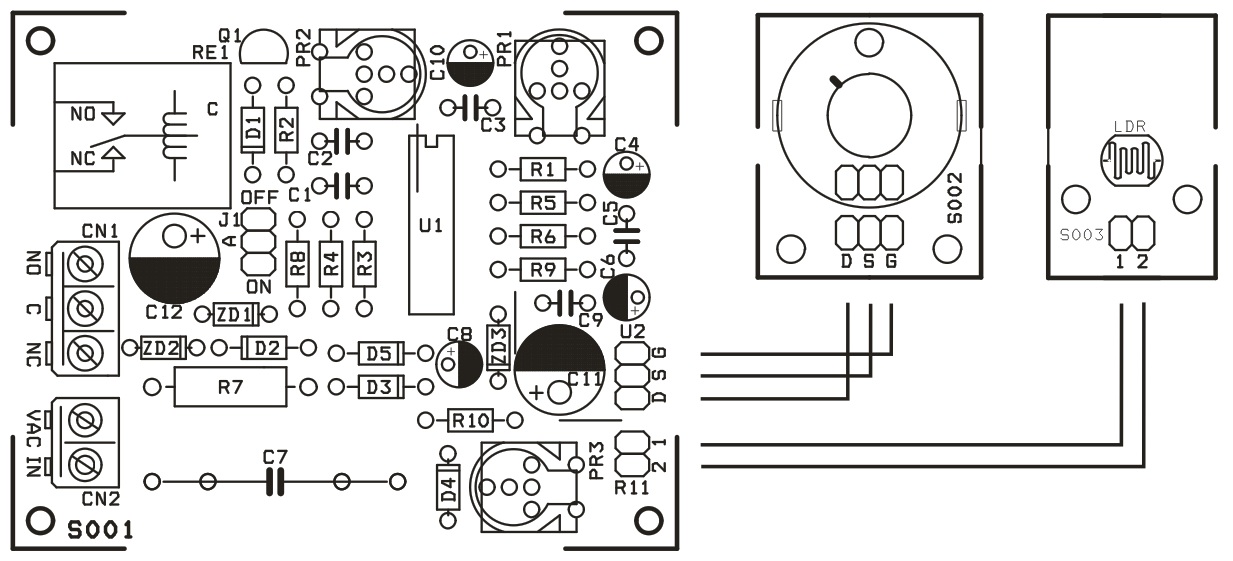
- J1 to Set the Mode
- PR1 to set the Sensitivity of the sensor
- PR2 to set the output Turn On Duration
- CDS R11 for Auto Day/Night detection
- (HIGH Voltage On Board) Do Not touch the PCB while power is on.
Schematic
Mode (Jumper J1):
This project offers three operating modes (ON, AUTO, OFF) which can be set through the MODE pin. While the chip is working in the AUTO mode the user can override it and switch to the TEST mode or manual ON mode, or return to the AUTO mode by switching the power switch. J1 Jumper is to set the desired modes.
| J1 Jumper | Operating Mode | Description |
| VDD | ON | Output is always On: Output is high RELAY ON |
| VSS | OFF | Output is Always Off: Output is low RELAY OFF |
| Open | Open | Outputs remain in the off state until activated by a valid PIR input trigger signal. When working in the AUTO mode, the chip allows override control by switching the ZC signal. |
CDS-LDR (Light Dependent Resistor):
CDS is a CMOS Schmitt Trigger input structure. It is used to distinguish between day time and night time. When the input voltage of CDS is high the PIR input is enabled. On the other hand, when CDS is low the PIR input is disabled. The input disable to enable debounce time is 5 seconds. Connect this pin to VDD when this function is not used. The CDS input is ignored when the output is active.
LDR Operations
| CDS PIN (LDR) | Status | PIR |
| Low | Day Time | Disabled |
| High | Night Time | Enabled |
LDR Operations
OSCD is an output timing oscillator input pin. It is connected to an external RC to obtain the desired output turn-on duration. Variable output turn-on durations can be achieved by adjusting variable resistor or setting various values of RC.
Power-on Initial
The PIR signal amplifier requires a warm up period after power-on. The input should be disabled during this period. In the AUTO mode within the first 10 seconds of power-on initialization, the circuit allows override control to enter the test mode. After 40 seconds of the initial time the chip allows override control between ON and AUTO. It will remain in the warm up period if the total initial time has not elapsed after returning to AUTO. In case that the ZC signal disappears for more than 3 seconds, the chip will restart the initialization operation. However, the restart initial time is always 40 seconds and cannot be extended by adding CRST to the RST pin as shown in the circuit.
The HT7610A offers mask options to select the output flash (3 times) when changing the operating mode. The output will flash 3 times at a 1Hz rate each time it changes from AUTO to another mode and flash 3 times at a 2Hz rate when it returns to the AUTO mode. However the output will not flash if the mode is changed by switching the MODE switch. Options for effective override: Once or twice Off/On operation of power switch within 3 seconds. Options for output flash to indicate effective override operation. Flash for the circuit.
Test mode control
Within 10 seconds after power-on, effective ZC switching will force the chip to enter the test mode. During the test mode, the outputs will be active for duration of 2 seconds each time a valid PIR trigger Signal is received. If a time interval exceeds 32 seconds without a valid trigger input, the chip will automatically enter the AUTO mode
Note:
- The output is activated if the trigger signal conforms to the following criteria:
- More than 3 triggers within 2 seconds
- A trigger signal sustain duration
- 0.34 seconds >/2 trigger signals within 2 seconds with one of the trigger signal sustain 0.16 seconds.
- The effective comparator output width is selected to be 24ms.
- The output duration is set by an external RC that is connected to the OSCD pin
Override control
When the chip is working in an AUTO mode (MODE=open), the output is activated by a valid PIR trigger signal and the output active duration is controlled by an OSCD oscillating period. The lamp can be switched always to ON from the AUTO mode by either switching the MODE pin to VDD or switching the ZC signal by an OFF/ON operation of the power switch (OFF/ON once or twice within 3 seconds by mask option). The term override refers to the change of operating mode by switching the power switch. The chip can be toggled from ON to AUTO by an override operation. If the chip is overridden to ON and there is no further override operation, it will automatically return to AUTO after an internal preset ON time duration has elapsed.
This override ON time duration is 8 hours. The chip provides a mask option to determine the output flash times (3 times) when changing the operating mode. It will flash 3 times at a 1Hz rate each time the chip changes from an AUTO mode to another mode or flash 3 times at a 2Hz rate when returning to the AUTO mode. But if the AUTO mode is changed by switching the MODE switch it will not flash.




May I know the model of the PIR sensor used in the circuit?
Your prompt response will be much appreciated. Thanks a lot in advance!
Another concern for the relay, what model of relay was used in the circuit?
I their any replace for the HT76140a Ic because i cant find this model of Ic
Please help me because I already bought all the components exect the IC and I’m having a hard time finding it and I’m using it for my project
You can find it on ebay.com or http://www.aliexpress.com
Please inform me another equivelent IC for this. Cannot find it.
It’s a discontinued IC but can be found online on ebay.com and http://www.aliexpress.com
is there any ckt diagram with biss0001 for pir
WITH SIMPLE OPAMP (DUAL 8 PIN OPAMP = use LM358) YOU CAN SET THE
In the AUTO mode within the first 10 seconds of power-on initialization, the circuit allows override control to enter the test mode : THIS CAN BE ACHIVED USING 10 SEC POR (Power On Reset) USING RC+D COMBO THEN TO 40106 (A) (THIS HAS 6 SCHMITTREGED STAGES), then to the control circuit. FOR LDR AVOIDING/TUNING USE OPAMP (B) STAGE IS REQUIRED. SIMILAR TO LDR, PIR OUTPUT CAN BE TUNED/TRIGGER LEVEL WITH OPAMP (A) with one more on delay with same R.C,D. AND ‘106 STAGE. WHEN THE PIR SIGNAL GOES OFF ONE OFF DELAY (4 SEC – OR MORE.FOR UPTO 10 SEC ADJUSTABLE DELAY INSTEAD OF R, PUT ONE 100K PRESET) CAN BE MADE RC+D(REVER TO THE FIRST SIMILAR STAGE). WITH 10K AND DIODE (w.r.t on/off delay the direction of diode will changed ) and after this one cap 100mfd/16 v; then one 40106(b) stage. the o/p of “b” will give a time delay of 1 sec. that’s it. then for final o/p s u can use 40106 (out of 4 balance stages) & any quad AND GATE. DRIVING RELAY WITH BC547 AS SHOWN.
FOR any clarification facebook / SKYPEE : SHIVKHUMAR; TWITTER: @SHIVKHUMAR. OR
EMAIL: hrd_comfort@yahoo.co.in
MDR SHIVKHUMAR MUDALIAR